Static Timing Analysis in FPGA
Static Timing Analysis in FPGA
- 7 min read
Static Timing Analysis in FPGA:
Certain design requirements must be met for an FPGA design to operate safely and without errors. One of the most important of these requirements is timing analysis.
Signals travelling from register to register inside the FPGA, from a register inside the FPGA to external hardware, or from external hardware to a register inside the FPGA must arrive within specific time windows. Timing analysis is the process of determining whether a design will operate reliably, based on the operating frequency defined in the constraint file and the fixed parameters of the target FPGA device.
Timing analysis is an essential step for guaranteeing the stable operation of a design. In a system that does not meet its timing requirements, signals may not be transferred from the source flip flop to the destination flip flop at the correct time, and unexpected behaviour may be observed.
Before moving on to the content of this article, the abbreviations used in the figures and in the text are explained below.
Tclk: The time spent on the path from the clock source to the clock input of the flip flop. It varies depending on the design.
tco (clock to output) or tcq (clock to q): The time elapsed between the rising edge of the clock signal arriving at the flip flop and the Q output. It is a fixed parameter related to the manufacturing technology.
Tdata: The time it takes for the data to travel from the Q output of the source flip flop to the D input of the destination flip flop. It varies depending on the design.
Jitter: The fluctuation of a signal, particularly at its transition instants.
Skew: The time delay caused by signal propagation.
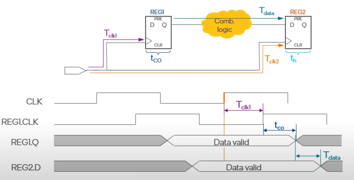
Figure 1: Representation of the abbreviations used on a timeline
Timing analysis examines whether the signal applied to the input of a flip flop inside the FPGA (the D input) changes within the permitted time window relative to the clock input. The analysis is carried out for two different time windows: the setup and the hold time requirements.
1. Setup time analysis:
A flip flop uses the rising edge of the clock signal to sample the signal applied to its input. It samples the D input at that rising edge and transfers it to the Q output.
In a real flip flop, the signal must remain stable for a certain period before the rising edge so that the sampling can be performed correctly. This period is called the setup time (tsetup). It is a fixed parameter related to the manufacturing technology. If the signal changes during this window, which lies immediately before the rising edge of the clock, the flip flop output enters a metastable, unstable state. In this unstable state the output of the flip flop fluctuates between 0 and 1, but after a certain amount of time it resolves and the output settles at a stable value.
Maximum allowed data path delay (for setup time) = Trequired_setup = tco + Tdata + tsetup (the pre-clock stability period required by the flip flop) + other factors (jitter, skew, etc.)
Trequired_setup must be ≤ Tclk.
In other words, rearranging the terms of the inequality, it can also be written as:
(tco + Tdata + tsetup) ≤ Tclk
The point to note here is that as the clock frequency increases, Trequired_setup decreases. Put differently, as the length of the designed data path increases, the achievable clock frequency decreases.
2. Hold time analysis:
The signal at the input of the flip flop must remain stable for a certain period after being sampled at the rising edge of the clock. This period is called the hold time (thold). It is a fixed parameter related to the manufacturing technology. If the signal at the D input of the flip flop changes during this window, the flip flop output enters a metastable, unstable state.
Minimum allowed data path delay (for hold time) = Trequired_hold = thold (the post-clock stability period required by the flip flop) + other factors (jitter, skew, etc.)
In other words, the time taken for the data to be generated at the source flip-flop and delivered to the destination flip-flop must be greater than or equal to the minimum hold time (plus the system uncertainties):
(tco + Tdata) ≥ Trequired_hold
The point to note here is that the clock frequency has no effect on Trequired_hold, because it is a parameter related to the sampling performed at the very same clock edge.
In short, setup and hold time checks verify the timing rules governing how long the signal must remain stable around the clock sampling instant. The time windows in which the signal at the flip flop input must stay stable, and in which it is allowed to change, are shown below.
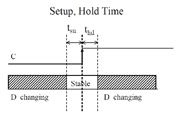
Figure 2: The time windows in which the flip flop input must remain stable and in which it may change(1)
Before covering how the setup and hold time calculations are performed, several examples are examined below in terms of whether they meet the setup and hold time requirements.
An example that is examined in terms of setup time and that operates without errors is shown in Figure 3 below.
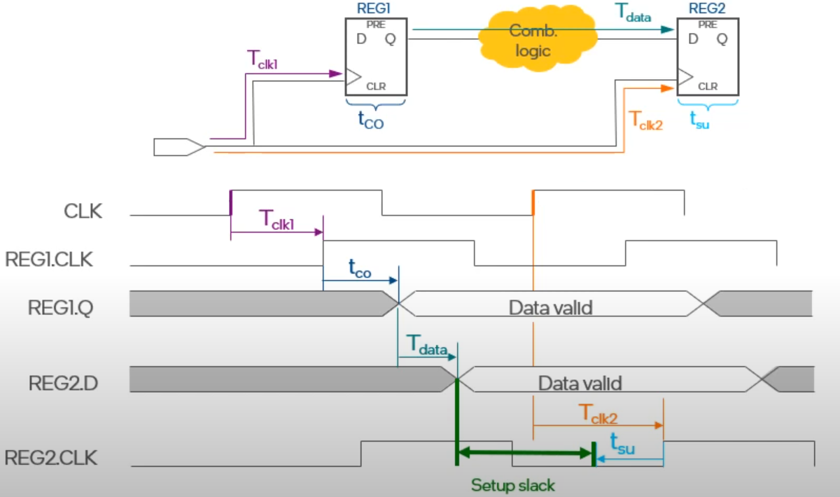
Figure 3: An example that operates without errors in terms of setup time
When the signals in the timing diagram are examined, it can be seen that once the REG1.Q signal leaving Register 1 arrives at the REG2.D input, more time than Tsetup remains before the next sampling instant. Therefore there is no violation in terms of setup time.
An example that is examined in terms of setup time and that contains a setup time violation is shown in Figure 4 below.
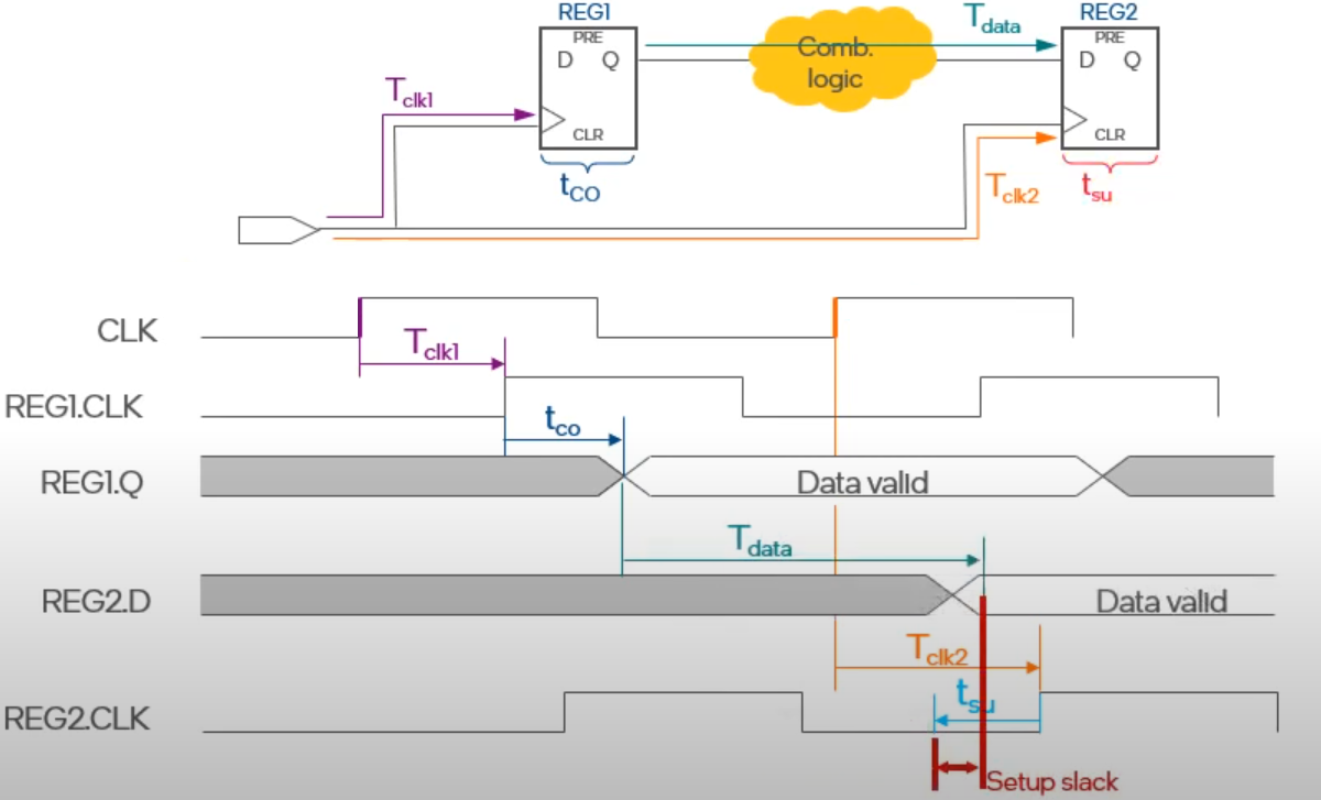
Figure 4: An example containing a setup time violation
When the signals in the timing diagram are examined, it can be seen that once the REG1.Q signal leaving Register 1 arrives at the REG2.D input, less time than Tsetup remains before the next sampling instant. The signal stability required before sampling is therefore not achieved, and a setup time violation occurs.
An example that is examined in terms of hold time and that operates without errors is shown in Figure 5 below.
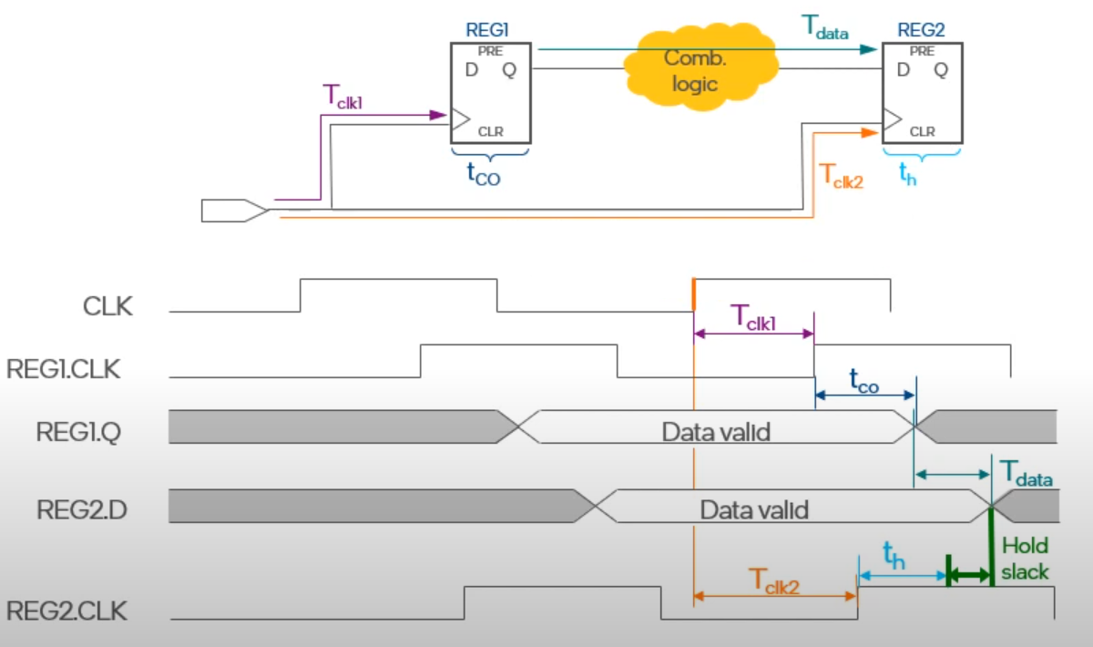
Figure 5: An example that operates without errors in terms of hold time
When the signals in the timing diagram are examined, it can be seen that after the REG1.Q signal leaving Register 1 arrives at the REG2.D input and is sampled on the next rising clock edge, it stays stable for longer than thold. Therefore there is no violation in terms of hold time.
An example that is examined in terms of hold time and that contains a hold time violation is shown in Figure 6 below.
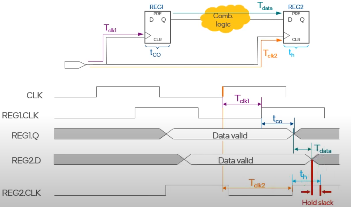
Figure 6: An example containing a hold time violation
When the signals in the timing diagram are examined, it can be seen that after the REG1.Q signal leaving Register 1 arrives at the REG2.D input and is sampled on the next rising clock edge, it stays stable for a shorter period than thold. The signal stability required after sampling is therefore not achieved, and a hold time violation occurs.
While performing setup and hold time analysis, the analysis tools calculate the slack (the amount of margin) for every data path. The parameters used in these slack calculations and the way they are computed are given below.
Setup Slack: Required data transfer time (for setup time) - Data arrival time ===> The data arrival time must be ≤ Trequired_setup.
Hold Slack: Data arrival time - Required data transfer time (for hold time) ===> The data arrival time must be ≥ Trequired_hold.
When the setup and hold slack values are positive, the design meets its timing requirements; otherwise the design contains a timing violation.
While positive setup and hold slack values guarantee the stable operation of the design, negative slack values can lead to metastability and unstable states in the system. This causes the outputs of flip flops to become unstable, causes other flip flops sampling those unstable flip flops to capture incorrect values, and can escalate into a failure that brings the whole system down. In a good design it is important to take these analyses into account in order to avoid such failures.
The content and figures in this article draw on the Understanding Timing Analysis in FPGAs video published on the Altera YouTube channel. (1): The figure is taken from vlsi-expert.