Reset Topologies in FPGA
Reset Topologies in FPGA
- 9 min read
In FPGA applications the reset architecture is extremely critical for the reliability of the design. Reset structures play a key role, particularly in space, aviation and other mission-critical systems, in quickly preventing possible faults and in defining the behaviour of the system at start-up.
In FPGAs there are two main reset structures: synchronous reset and asynchronous reset.
A synchronous reset clears the registers in step with the clock signal. Its advantages are as follows:
- Since it takes effect synchronously, it does not cause timing violations.
- It is advantageous in terms of timing violations.
- It is immune to glitches on the reset input. Its disadvantages are as follows:
- It requires a clock signal. It cannot work without a clock.
- After being asserted, it needs a delay of one clock period to take effect.
- It may require additional FPGA resources.
- It creates a large fanout inside the FPGA.
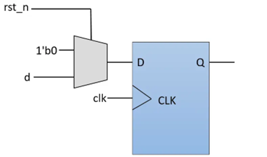 Figure 1 - Synchronous reset structure
An asynchronous reset clears the flip-flops independently of the clock signal. It is applied through the reset input of the flip-flops. Its advantages are as follows:
- Since it does not require a clock signal, it can be triggered at any instant.
- Its effect takes place with very little delay after being asserted.
- It requires fewer FPGA resources than a synchronous reset. Its disadvantages are as follows:
- There is a high probability of a timing violation at the moment of its release.
- It is sensitive to glitches on the reset input.
The two reset structures have different advantages and disadvantages. In most applications an asynchronous reset is commonly used during power-on, whereas a synchronous reset is preferred during normal operation. When a synchronous reset signal arrives, the clearing takes place in step with the clock signal. The outputs of the relevant flip-flops can therefore be changed at the correct time, without violating the timing rules required for stable operation. An asynchronous reset signal, on the other hand, can occur at any instant independently of the clock, so it may violate the timing rules, create metastability and push the FPGA into an unstable state. This situation can be examined in Figure 2.
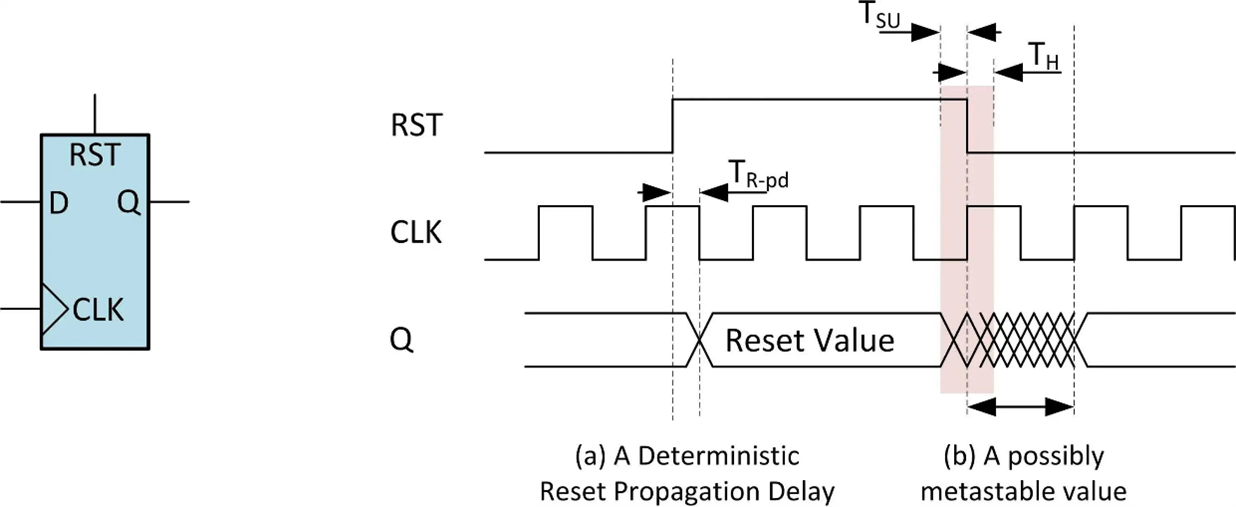 Figure 2 - Timing violation caused by an asynchronous reset
Examining Figure 2, it can be seen that when the asynchronous reset signal arrives, the clearing takes place independently of the clock signal. After the asynchronous reset is released, the registers return to normal operation and are updated with new values in step with the clock. In order for these new values to be propagated to the output correctly, that is, without a timing violation, the signal must remain stable for Tsetup before the output value changes and for Thold after it changes. In case a, on the left-hand side of the figure, the clearing complies with these timing rules. If the reset signal arrives between these two windows, the output value is changed by the effect of the reset signal and, since it cannot remain stable throughout the required interval, a timing violation occurs. In case b, on the right-hand side of the figure, the clearing does not comply with these rules and a timing violation occurs.
In large designs, routing delays that arise while distributing the reset signal can combine with the cause described above and lead to timing violations. When an asynchronous reset signal arrives, the clearing is performed without waiting for any clock signal. An asynchronous reset should be used especially when a faulty system state is detected and the outputs must be forced to a safe value quickly. In addition, when there is no clock signal, such as at power-up, an asynchronous reset is mandatory in order to clear all registers and output values.
Since both structures have their own advantages and disadvantages, a hybrid approach should be used in space, aviation and other critical applications. In this hybrid approach it is recommended to use an asynchronous reset at power-on and a synchronised reset during normal operation, replicated with a Triple Modular Redundancy structure according to how critical the application is. Example circuits and the recommended structures are given below.
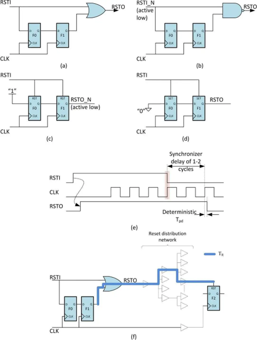 Figure 3 - Reset synchroniser circuits
Circuits a and b in Figure 3 are asynchronously asserted, synchronously de-asserted synchroniser circuits for active-‘1’ and active-‘0’ resets respectively. The logic gate at their output is driven active by the reset signal independently of the clock. The other input of the logic gate is the output of flip-flop F1, which is clocked synchronously. Flip-flop F0, driven by the asynchronous reset input, is connected to the input of F1. F0 passes the input signal to F1 in step with the clock, and F1 in turn drives the logic gate. When the reset signal is released, the reset output is held active for as many clock cycles as there are flip-flops, and once that period is complete it is de-asserted synchronously with the clock. In this way the reset can be asserted asynchronously and de-asserted synchronously. The cascaded flip-flops in this structure prevent metastability. It should not be forgotten that, because of the cascaded flip-flops, these circuits will keep the reset output active for as many clock cycles as there are flip-flops after being triggered.
Circuits c and d in Figure 3 are synchroniser circuits made up of cascaded flip-flops, triggered by active-‘1’ and active-‘0’ reset signals respectively. These circuits synchronise the incoming asynchronous signals to the clock and pass them to the output. Unlike structures a and b, there is no asynchronous assertion; they operate purely synchronously with the clock. The cascaded flip-flops in this structure prevent metastability.
Using the reset outputs produced by the structures above throughout an entire design causes timing and routing problems, especially in large designs. To solve the timing part of this problem, many parallel flip-flops can be added to the output synchroniser circuit as shown in Figure 4, which brings the design into compliance in terms of timing.
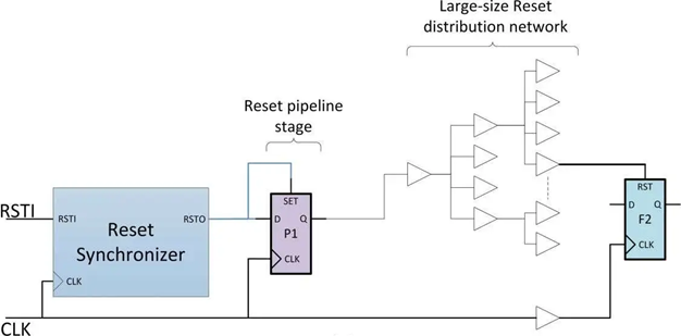 Figure 4 - Circuit that makes the synchroniser compliant in terms of timing
Because the circuit in Figure 4 uses the asynchronous set feature, no clock cycle is lost while the reset is being asserted. After the assertion ends, a one-clock delay appears at the output. When this structure is placed close to the modules the reset signal has to reach, the path carrying the reset signal becomes shorter and routing-related timing problems can be avoided. When designing the reset architecture of a design with multiple clock domains, a separate reset structure must be used for every clock domain. Synchronising the asynchronous reset separately to each clock domain, according to that domain’s own clock frequency, is necessary in order to avoid metastability.
Power on Reset structure:
Especially in flash-based FPGAs, the initial values of the registers may not be set correctly at start-up. To prevent this, an asynchronous reset is applied for a certain period from the moment power is first applied, so that all registers in the design are cleared and their initial values are set as intended. In addition, some time must be allowed for the supply voltage and for the PLL (and similar) clock structures to reach a stable regime.
For this purpose, either the POR structure that vendors add in hardware or a POR structure designed at RTL level can be used. The purpose of the POR structure is to apply a reset signal unconditionally for a certain period, only at start-up. This guarantees that all registers take their intended values during power-up. Once the POR period expires, the system moves into normal operation.
The POR becomes active the moment power first reaches the FPGA. At that instant the clock signal is usually either absent or not yet stable, so the POR performs the reset through an asynchronous reset output. Once the desired timeout completes, it is de-asserted synchronously with the clock signal.
The lock signal of the FPGA clock IP cores is generally used to start the timer used for the POR. This signal is asserted by the IP core once the clock distribution unit inside the FPGA starts producing a stable output, and it stays asserted as long as the clock remains stable.
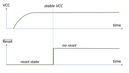 Figure 5 - De-assertion of the POR over time
Triple Modular Redundancy (TMR) structure:
In critical applications such as space or aviation projects, a TMR structure can be used so that internal signals affected by external factors (SEU and radiation) do not produce erroneous outputs. In this structure (although it varies with the TMR architecture) the signal to which TMR is applied is synthesised in triplicate and routed to the target structure. At the final stage a voter compares the input signals, and the state shared by at least two of the three signals is chosen as the output. As a result, an error can only occur if at least two of the three signals are corrupted. The block architecture of the TMR structure is given in Figure 6.
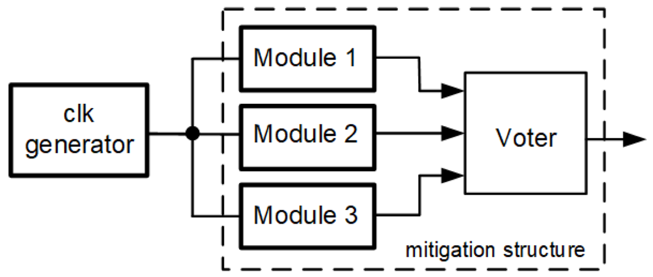 Figure 6 - TMR structure
The TMR option can be enabled with an attribute added to the RTL code. It is also applied automatically in the reset structures of rad-hard FPGAs used for space applications.
The VHDL attribute code is given below:
	--Xilinx
	attribute TMR : string;
	attribute TMR of my_ff : signal is "TRUE";
	--Microchip
	attribute tmr : string;
	attribute tmr of my_ff : signal is "ENABLED";
The Verilog attribute code is given below:
	--Xilinx
	(* TMR = "TRUE" *) reg my_ff;
	(* TMR = "TRUE" *) wire my_reset;
	--Microchip
	(* tmr = "ENABLED" *) reg my_ff;
	(* tmr = "ENABLED" *) wire rst_n;
Glitch filtering:
In sensitive applications it is recommended to use a glitch filter structure in order to reduce the glitch sensitivity that is one of the disadvantages of the asynchronous reset. A glitch filter prevents the reset input from becoming active because of a very short disturbance. This gives the asynchronous reset signal immunity against noise and environmental effects, which is especially valuable in critical designs.
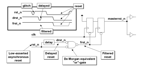 Figure 7 - Glitch filter
In the reset glitch filter shown in Figure 7, the input signal itself and a slightly delayed copy of it are applied to an or gate (or an and gate for an active-‘0’ reset). Delaying the input signal can be done with the hardware macros provided by the vendors or by creating a delay with simple logic. Since the gate receives both the glitched signal and the copy the glitch has not yet reached, an unaffected output is obtained; this filtered signal is then fed into the synchroniser circuit and brought into synchronism with the clock. The operation of the filter can be understood by examining the waveforms at the top left: the glitch-affected rst_n, the delayed drst_n and the filtered frst_n.
In conclusion, synchronous and asynchronous reset structures are two different approaches, each with its own advantages and disadvantages. Using them together improves the reliability of the design and brings the strengths of both into the same architecture, which is particularly important in critical applications such as space and aviation.
The following sources were used while preparing this article: VLSIVerify - DFF with synchronous reset, Embedded - Asynchronous reset synchronization and distribution challenges and solutions, Asynchronous & Synchronous Reset Design Techniques - Part Deux and Xilinx - UG949.